Fabrication and characterization of semiconductor micro-tubes and micro-plates on GaAs substrate
The ongoing project is being executed by Dr. S. Sarvanan, Professor and Head, Centre for Photonics and Nanotechnology, from Sona College of Technology, Salem, Tamilnadu.
The project aims to Fabricate the micro tubes and plates on GaAs substrates, Optimize the sacrificial layer etching,Design and fabricate the photomask, Characterize those fabricated structures by SEM, Micro PL and Micro Raman.
Semiconductor micro tubes and micro plates will be fabricated by using III-V compounds semiconductor. The method is based on the concept of the strain-induced three-dimensional micro and nano structuring, the designing of various epitaxial strained structures by changing the thickness of InGaAs and GaAs layers and composition of InGaAs layer. Then, the epitaxial layers will be grown in ultra high vacuum environment on GaAs (001) oriented substrates. Fabrication of micro tubes by etching the sacrificial layer in the optimized selective etchant. Such micro-and nano-structures using compound semiconductors are expected to be applied to develop novel photonic devices.
The fabrication of the micro-tube is a complex task that requires many process steps. The most popular technology of surface micro machining that can be exhibits complex engineering, manual assembly, poly crystalline components, and complex of hinge fabrication. The new technology of self assembly mechanism has been introducing single crystalline components easy to integrate with optoelectronic devices. The selective etching rate of the sacrificial layer will be optimized by varying the composition of HF and H2O. If the etching is too fast then the tubes may break when it rolls fast. So, the HF and H2O mixing ratio has to be optimized. The epilayer will be rolled by the strain relaxation of InGaAs when the structure selectively etched in optimized HF and H2O mixture. After releasing, to avoid collapse of the free-standing structures owing to capillary forces, the HF-based etchant will be replaced successively, with water and methonal. Finally, the diameter of the rolled tube will be measured by Scanning Electron Microscope (SEM).

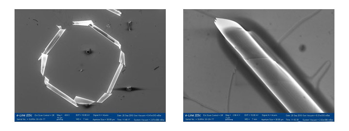
The microtubes formed by self assembling techniques were observed by Scanning Electron Microscope (SEM). Also, the Photoluminescence and Micro Raman spectras of the Double quantum well were observed.